|
|
|
|
|
|
|
|
|
|
|
|
|
University
of Latvia, Department of Physics
Research working group |
|
|
|
|
|
|
|
|
|
|
|
|
|
Actuality |
|
|
|
|
|
|
|
|
|
|
|
|
|
|
|
|
|
|
Multiphysics
in Crystal Growth
- mathematical modelling |
|
|
|
|
|
|
|
|
|
|
|
|
|
|
|
|
|
|
Former workshop in June 2002 |
|
|
Location:
Zellu str 8, Riga, LV-1002, Latvia |
|
|
|
|
|
|
|
|
|
|
|
|
|
|
|
|
|
|
|
|
|
|
|
|
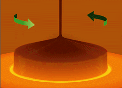
Research field:
Mathematical modelling of various physical aspects of industrial and
research crystal growth on the macroscopic and atomic level.
(see research field) |
|
|
|
|
|
|
|
|
|
|
|
|
 |
|
|
|
Contact person:
Dr. Phys. Andris Muiznieks (see contacts)
|
|
|
|
|
|
|
|
|
|
|
|
|
|
|
|
|
Team:
Experienced scientists on the field of mathematical modelling of HD,
EM and thermal processes:
4 Dr.-Phys., at the moment 2 doctor (phd) students, some students.
|
|
|
|
|
|
|
|
|
|
|
|
|
|
|
|
|
Cooperation partners:
The main partner for international cooperations is the Institute for
Electrothermal Processes, University of Hanover, Germany (Wilhelm
Busch Str. 4, 30167 Hanover, Prof. Bernard Nacke, Prof. Alfred Muehlbauer).
International cooperations of our working group
with various companies and academic partners are mainly running
through the Institute for Electrothermal Processes, e.g. Wacker
Siltronic AG (Burghausen, Germany), Institute for Crystal Growth
(Berlin, Germany) a.o.
|
|
|
|
|
|
|
|
|
|
|
|
|
|
|
|
|
design
by @mihy |
|
|
|
|
|
|
|
|
|
|
|
|
|
|
|
|
|
|
|
|
|
|